
In today’s tech-driven world, understanding how to fabricate printed circuit boards (PCBs) is essential for anyone looking to create electronic devices. This article explores the step-by-step process of PCB fabrication, from design to assembly, highlighting key techniques and tools involved. Whether you’re a hobbyist or a professional, mastering PCB fabrication can improve your projects and boost your skills in electronics.
Understanding PCB Fabrication
PCB fabrication refers to the process of creating printed circuit boards, essential components in electronics. This process transforms electronic designs into physical structures, allowing for the assembly of electronic components.
What Is PCB Fabrication?
PCB fabrication includes several key steps to construct circuit boards that support electronic components. It starts with a design, typically created using specialized software, which defines the layout and circuitry of the board. The design then undergoes manufacturing processes such as etching, drilling, plating, and solder masking. Each step contributes to crafting a reliable board, capable of conducting electricity while fitting within specific physical constraints.
Importance of PCB Fabrication
PCB fabrication plays a critical role in modern electronics, influencing performance and reliability. High-quality fabrication ensures electrical connections can withstand operational stress, preventing failures in devices. Additionally, effective fabrication reduces production costs and time, enhancing efficiency for manufacturers. Understanding this process helps engineers and hobbyists create functional circuit boards tailored to their specific needs, fostering innovation in electronics design and development.
Materials Required for PCB Fabrication
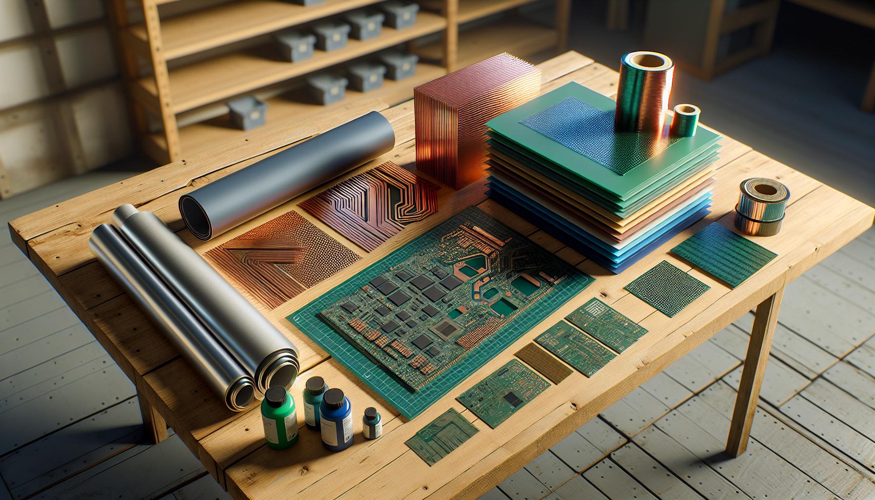
PCBs require specific materials to ensure effective functionality and durability. Understanding these materials facilitates efficient fabrication.
Types of Materials
- Substrate Materials: Commonly used substrates include FR-4 (a glass-reinforced epoxy laminate), CEM-1, and flexible polyimide. These materials provide the necessary support and electrical insulation.
- Conductive Materials: Copper foil functions as the primary conductive material, crucial for creating pathways for electrical signals.
- Solder Mask: A polymer layer, solder mask protects circuit traces from short circuits and oxidation. It also helps delineate soldering areas.
- Silkscreen Ink: This ink allows for printing labels and symbols on the PCB, enhancing usability and maintenance.
- Design Software: Tools like Eagle or KiCAD allow for schematic capture and PCB layout design, providing a digital framework for fabrication.
- Etching Equipment: Ferric chloride or other etchants require precise handling for effectively removing copper from the PCB.
- Drilling Equipment: A CNC machine or manual drill facilitates drilling holes for components and vias, essential for connectivity.
- Soldering Iron: A well-calibrated soldering iron enables accurate component placement and secure connections.
- Testing Tools: Multimeters and oscilloscopes verify electrical functions and performance post-fabrication, ensuring reliability.
Understanding these materials and tools provides a solid foundation for successful PCB fabrication.
The PCB Fabrication Process
The PCB fabrication process involves multiple critical steps to transform electronic designs into functional printed circuit boards.
Designing the PCB
Designing the PCB begins with creating an electronic schematic using specialized software like Eagle or KiCAD. This schematic represents the electrical connections between components. Designers must ensure the layout adheres to design rules, encompassing trace width, clearance, and component placement. Accurate designs facilitate optimal signal integrity and functionality.
Creating the PCB Layout
Creating the PCB layout translates the schematic into a physical representation. The layout encompasses component positions, traces, and vias. Designers utilize layout tools to manage signal pathways effectively, ensuring they minimize interference and maintain impedance control. Completing this step involves verifying the design through design rule checks (DRC) to identify and rectify potential issues.
Etching the PCB
Etching the PCB involves removing unwanted copper from the substrate to create the desired circuit pattern. This process typically employs chemical etchants like ferric chloride or ammonium persulfate. First, a photoresist layer is applied, followed by exposure to ultraviolet light through a photomask. After the etching solution removes the exposed copper, the photoresist is stripped away, revealing the finished circuit pattern. Proper etching achieves precise traces necessary for effective conductivity and performance.
Testing and Quality Assurance
Testing and quality assurance play crucial roles in ensuring the reliability and functionality of printed circuit boards (PCBs). A thorough testing process identifies defects early, preventing costly errors in electronic devices.
Importance of Testing
Testing ensures that PCBs function correctly and meet specified performance standards. It validates design accuracy and confirms that all connections are intact. By identifying issues early, testing reduces the risk of failures in the final product. Consistent testing enhances overall reliability and prolongs the lifespan of electronic devices.
- Visual Inspection: Inspecting PCBs visually helps identify obvious defects such as solder issues, component misplacement, and physical damage.
- Electrical Testing: Conducting electrical tests verifies that the circuits operate as designed. Methods include:
- Continuity Testing: Checks for uninterrupted electrical paths.
- Functional Testing: Evaluates the overall operation of the PCB in the intended application.
- Automated Optical Inspection (AOI): This method employs cameras and computer algorithms to detect defects during the manufacturing process.
- In-Circuit Testing (ICT): Analyzing individual components and their connections in the PCB using specialized test fixtures identifies faulty components.
- Thermal Imaging: Using infrared cameras to detect heat patterns assists in identifying overheating components or areas with poor connections.
Tips for Successful PCB Fabrication
Effective PCB fabrication relies on adherence to best practices while avoiding common pitfalls. These tips ensure a streamlined process and improve the quality of the final product.
Best Practices
- Select Appropriate Materials: Choose high-quality substrate materials like FR-4 for durability. Ensure that copper foil thickness meets the project’s current carrying requirements.
- Utilize Design Software Efficiently: Use specialized software, such as Eagle or KiCAD, to create accurate designs. Follow design rules to maintain signal integrity and avoid errors.
- Implement Proper Etching Techniques: Choose chemical etchants that provide precise results and minimize waste. Control etching duration to ensure the copper traces are appropriately etched without damaging the substrate.
- Conduct Comprehensive Testing: Employ a variety of testing methods, including visual inspection and continuity testing, to detect defects early. Implement Automated Optical Inspection (AOI) to identify minute errors.
- Maintain Clean Work Environments: Keep the workspace clean to avoid contamination of materials. Regularly clean tools and equipment to ensure the integrity of the PCB fabrication process.
- Document Every Stage: Record each step of the process for future reference. This aids in troubleshooting and improves the consistency of subsequent fabrications.
- Neglecting Design Rules: Failing to adhere to established design rules can lead to connection failures and signal integrity issues. Ensure compliance with all applicable standards.
- Using Inadequate Testing: Skipping thorough testing increases the chance of undetected defects. Implement rigorous testing protocols to validate each PCB before use.
- Overlooking Production Tolerances: Not considering manufacturing tolerances can result in assembly problems. Always account for tolerances in the design phase.
- Ignoring Environmental Factors: Failure to consider temperature and humidity during storage and fabrication can affect the quality of materials. Control these factors to optimize manufacturing conditions.
- Underestimating Layout Complexity: Simplifying designs can lead to a loss of functionality. Ensure that all components are optimally placed to achieve desired performance.
- Rushing the Process: Hurrying through any part of the fabrication process can lead to mistakes. Allocate sufficient time for each phase to ensure a high-quality outcome.
Conclusion
Mastering PCB fabrication is essential for anyone involved in electronics. With a solid understanding of the processes and materials involved, individuals can create reliable and efficient circuit boards. By following best practices and avoiding common pitfalls, they can improve their projects and contribute to innovation in the field.
The journey from design to testing requires attention to detail and a commitment to quality. As technology continues to evolve, the skills gained in PCB fabrication will remain invaluable, empowering creators to push the boundaries of what’s possible in electronic design.
Frequently Asked Questions
What is PCB fabrication?
PCB fabrication is the process of turning a printed circuit board design into a physical board that can hold electronic components. It involves various manufacturing steps, including etching, drilling, and assembling layers to create the necessary electrical connections.
Why is PCB fabrication important?
PCB fabrication is crucial for transforming electronic designs into reliable hardware. It ensures that components function correctly, withstand stress, and maintain performance, ultimately leading to better product quality and reduced production costs.
What materials are used in PCB fabrication?
Common materials for PCB fabrication include substrate materials like FR-4 and CEM-1, copper foil for electrical connections, and solder masks for protecting the circuitry. These materials contribute to the board’s durability and functionality.
Which tools are essential for PCB fabrication?
Essential tools for PCB fabrication include design software like Eagle or KiCAD, etching and drilling equipment, soldering irons, and various testing tools. These tools help designers and manufacturers create PCBs effectively and efficiently.
What steps are involved in the PCB fabrication process?
The PCB fabrication process typically involves several steps: designing the circuit using specialized software, creating the physical layout, etching unwanted copper, drilling holes for components, and finally assembling everything together.
How can I ensure successful PCB fabrication?
To ensure successful PCB fabrication, select high-quality materials, utilize design software effectively, conduct thorough testing throughout the process, maintain a clean workspace, and document each step for future reference.
What common pitfalls should I avoid in PCB fabrication?
Common pitfalls in PCB fabrication include neglecting design guidelines, using inadequate testing methods, overlooking production tolerances, underestimating layout complexity, and rushing through the fabrication process, which can lead to defects and reduced performance.
How is PCB testing conducted?
PCB testing involves validating the design and ensuring all connections are intact. Common methods include visual inspection, electrical testing (continuity and functional testing), Automated Optical Inspection (AOI), In-Circuit Testing (ICT), and thermal imaging for identifying issues.